SEMICONDUCTORS: THE BASICS OF ALL ELECTRONICS AND INVENTIONS #5
stemng·@oluwabori·
0.000 HBDSEMICONDUCTORS: THE BASICS OF ALL ELECTRONICS AND INVENTIONS #5
Series of this write-up on the fabrication of semiconductor devices such as Integrated circuits, transistor, diode e.t.c was started in the last episode of "SEMICONDUCTORS: THE BASICS OF ALL ELECTRONICS AND INVENTIONS" where I was able to take us through the various processes and methods involved in the production of an electronic grade silicon(EGS), also I stated reasons why SiHCl3 was predominantly used in synthesis of EGS rather than pyrolysis method. Today's episode shall entails all processes involved in the manufacturing of Single crystal Silicon from an electronic Grade Silicon (EGS).  [Electronic device processing plant](https://www.bbsautomation.com/solutions/electronic-devices) Here we go! Remember to visit [episode 1](https://steemit.com/stemng/@oluwabori/semiconductors-the-basics-of-all-electronics-and-inventions), [episode 2](https://steemit.com/stemng/@oluwabori/semiconductors-the-basics-of-all-electronics-and-inventions-2), [episode 3](https://steemit.com/stemng/@oluwabori/semiconductors-the-basics-of-all-electronics-and-inventions-3) and [episode 4](https://steemit.com/stemng/@oluwabori/semiconductors-the-basics-of-all-electronics-and-inventions-4) of this write-up. # How to manufacture Single crystal Silicon from an electronic Grade Silicon (EGS) Single crystal Silicon can be manufactured by converting Electronic grade silicon (EGS) also called polycrystalline EGS into a single crystal ingot, which are used to obtain the final wafers. This can be achieved through two main techniques. 1. **Czochralski technique (CZ)** - this is the dominant technique for manufacturing single crystals. It is especially used for manufacturing large wafers that are currently used in IC fabrication. 2. **Float zone technique** - this is mainly used for the production of small sized wafers. The float zone technique is suited for producing specialty wafers that contain low oxygen impurity concentration. Lets look into the two techniques one after the other. # Czochralski crystal growth technique A schematic of this growth process is shown below. <center>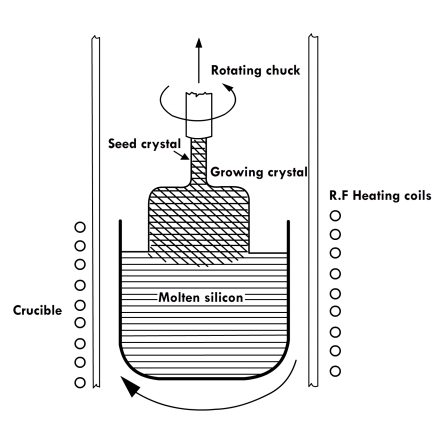 Schematic of the Czochralski growth technique [Adapted from Electronic materials, devices, and fabrication](http://nptel.ac.in/courses/113106062/Lec21.pdf)</center> **The various components of the process are:** 1. Furnace 2. Crystal pulling mechanism 3. Ambient control - atmosphere 4. Control system circuitry # Functions of various component of the growth apparatus The furnace consists of a crucible, crucible support known as a susceptor, rotational mechanism, heating element and power supply, and a chamber. The crucible is the most important component of the growth apparatus because it contains the melt. The crucible should be made with material that are chemically unreactive with molten silicon and must have high melting point, thermal stability, and hardness. The suitable materials for crucible are silicon nitride (Si3N4) and fused silica (SiO2), which satisfy the required properties. The susceptor serves as a support for the silica crucible. Graphite is the material of choice for the susceptor because of its high-temperature properties which is provided for better thermal conditions. The graphite must also be pure to prevent contamination of the crystal caused by impurities that can be introduced by a volatilized graphite at the temperature involved. The susceptor rests on a pedestal whose shaft is connected to and powered by a motor that provides rotation. It is necessary that the crystal growth is conducted in an inert gas (argon or helium) or vacuum because of the following reasons: - The hot graphite parts must be protected from oxygen so that erosion can be prevented. - The gas around the processing plant must not react with the molten silicon. The above requirements are met in vacuum growth. <center>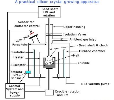 [Adapted from circuitstoday](http://www.circuitstoday.com/silicon-substrate-preparation)</center> # Procedure of the Czochralski crystal growth technique The starting material for the CZ process is electronic grade silicon (EGS), which is melted in the furnace. , The electronic grade silicon with an appropriate amount of dopant are put into a quartz crucible, which is then placed inside a crystal growth furnace to be processed, since monolithic ICs are usually fabricated of manufactured on a substrate which is doped with impurity. The material is then heated to a temperature above 1500 ◦C which is slightly in excess of the silicon melting point of 1420 degree Celsius. A small single-crystal rod of silicon called a seed crystal with the desired orientation of the final wafer is then dipped into the silicon melt. Once silicon is made in contact with the seed crystal, the conduction of heat that takes place in the system makes the seed crystal to produce a reduction in temperature of the melt slightly below the melting point of silicon. Therefore the silicon freezes onto the end of the seed crystal, and as the seed crystal is slowly pulled up by the crystal pulling mechanism out of the melt, a solidified mass of silicon is pull up with it which is a crystallographic continuation of the seed crystal. To produce crystalline ingots of circular cross section, both the seed crystal and the crucible are rotated in opposite directions to each other during the crystal pulling process so as to ensure uniformity across the surface, therefore the liquid solid interface remains near to the surface of the melt if the pulling rate and temperature are correctly chosen. Several hours are required for the “pulling” of a complete ingot. To prevent oxidation and to reduce gaseous impurities, the crystal pulling must be done in an inert-gas atmosphere such as argon or helium, and also, a vacuum is used. Crystal pulling are carefully controlled because the pull-rate is closely related to the heat input and losses, crystal properties and dimensions. Also, the diameter of the ingot is controlled by the pulling rate and the melt temperature producing a long single crystal silicon with ingot diameters of about 100 to 150 mm (4 to 6 inches) being the most common. To create doped crystals, the dopant material is introduced into the Si melt so that it can be incorporated in the growing crystal. There is a feedback system that control this process such that the melt temperature is monitored with a thermocouple and feedback controller. # Float zone technique <center>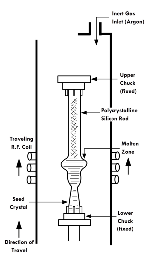 Schematic of the float zone technique [Adapted from Electronic materials, devices, and fabrication](http://nptel.ac.in/courses/113106062/Lec21.pdf)</center> The float zone technique is used for small wafer production, containing low oxygen impurity. The electronic grade silicon (EGS) rod is fused with the single crystal seed, this is then melted along the length of the rod by a traveling radio frequency (RF) coil in an inert gas furnace. The RF coil starts from the fused region, containing the seed, and travels up towards the upper chunk. When the molten region solidifies, it has the same orientation as the seed. To reduce gaseous impurities, the furnace is filled with an inert gas like argon. Also, oxygen ’free’ Si wafers are produced since no crucible is used. This process produces large number of dislocations so it will be difficult to extend this technique for large wafers, but it is suited for small specialty applications requiring low oxygen content wafers. <center> [Measuring single-crystalline silicon ingots](https://www.homepower.com/articles/solar-electricity/equipment-products/peek-inside-pv-cell)</center> # Ingot Trimming and Slicing After the single crystal (ingot) is obtained following the above processes, there is need for it to be further processed to produce the wafers. Therefore, the wafer is to be shaped and cut using industrial grade diamond tipped saws. The shaping operations involve two steps: the extreme top and bottom portions of the ingot are cut off and the ingot surface is grounded to produce a constant and exact required diameter, usually 100,125, or 150 mm. The ingots are checked for resistivity and orientation. Resistivity check is done by a four point probe technique which is used to confirm the dopant concentration while the orientation is measured by x-ray diffraction at the ends (after grinding).The ingot is then sliced to produce flat circular slices or wafers that are about 600 to 1000 micro meters thick using a large-diameter stainless steel saw blade with industrial diamonds. There are two types of flats to be produced: 1. Primary flat – Primary flat is grounded relative to a specific crystal direction. This is used as a visual reference to the orientation of the wafer produced. 2. Secondary flat – Secondary flat is used to identify the wafer, dopant type and orientation. Inner diameter (ID) slicing is the most commonly used technique. <center>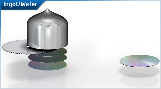 [ Slicing of ingot](https://blogs.intel.com/jobs/files/2012/02/S2S_2.png)</center> # Wafer Polishing and Cleaning The next after cutting is that the wafers are chemically etched so as to remove any damaged and contaminated regions. The mixture of hydrofluoric acid, nitric acid, and acetic acid is used as the etching material. After etching, polishing of damaged surfaces of the sliced ingot is very necessary because of the following reasons. • To improve the parallel of the ingot slice • Removal of the damaged silicon surface that is caused due to the sawing process. • To produce a highly planar flat surface required for the photo-lithographic process especially when it involves flue-line geometries. The surfaces are first polished using a rough aluminium abrasive powders of decreasing grit size (down to a final 1 micro meters diameter), followed by a chemical mechanical polishing (CMP) procedure. CMP involves using a slurry of fine SiO2 particles suspended in aqueous NaOH solution. The pad is usually a polyester material. Polishing happens both due to mechanical abrasion and also reaction of the silicon with the NaOH solution that makes the wafer into a mirror like finishing. <center>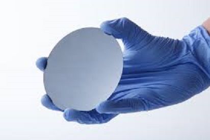 [Single crystal silicon](https://www.pi-kem.co.uk/shop/product/2-inch-test-grade-silicon-wafers-nphos-25-pack)</center> After the wafer polishing operations have been completed, the wafers are gently and thoroughly cleaned, and then dried. They are now ready to be used for the various processing steps such as photolithography and diffusion which will be described in the subsequent series of this write-up. _Thanks for your time Don't miss the next episode_ References [Ref 1](http://www.circuitstoday.com/ic-fabrication-techniques) [Ref 2](http://www.circuitstoday.com/silicon-substrate-preparation) [Ref 3](https://www.google.com.ng/url?sa=t&rct=j&q=&esrc=s&source=web&cd=2&cad=rja&uact=8&ved=0ahUKEwjg5b3r_sjYAhWMJMAKHZGTDcAQFgguMAE&url=https%3A%2F%2Fcnx.org%2Fexports%2F6c6beb3d-3f4b-4383-85d3-9ad52ee84251%403.pdf%2Fsemiconductor-grade-silicon-3.pdf&usg=AOvVaw2qC9wBacafAVX2md0pDxqd) [Ref 4](http://www.circuitstoday.com/ic-fabrication-techniques) [Ref 5](https://www.linkedin.com/pulse/comparison-different-methods-manufacturing-electronic-jayant-sidhu) [Ref 5](http://nptel.ac.in/courses/113106062/Lec21.pdf)
👍 oluwabori, bat-junior, venzy, greenrun, rubies, bikkichhantyal, zapper, steemstem, dna-replication, curie, lafona-miner, liberosist, meerkat, anwenbaumeister, hendrikdegrote, kushed, pharesim, rayken04, timsaid, thevenusproject, alexander.alexis, ovij, mrs.agsexplorer, lemouth, mobbs, somethingburger, kedi, ongoingwow, geekpowered, jamhuery, fancybrothers, tormiwah, sco, steemedia, teofilex11, bp423, diggerdugg, vl248, toxichan, cebymaster, dickturpin, gamesjoyce, cotidiana, anarchyhasnogods, kharrazi, the-devil, foundation, lamouthe, rachelsmantra, nitesh9, kerriknox, gra, rjbauer85, pearlumie, amavi, dber, justtryme90, gentleshaid, mystifact, kenadis, carloserp-2000, mountainwashere, hadji, teamhumble, walkinharmony, steemulator, mcyusuf, ubg, kingswisdom, himal,